[Semiconductor Device Characterization]
♦ Device fabrication - MOS devices - High-k capacitors (DRAM & Flash) - Oxide semiconductor transistors - OLEDs
|
[Semiconductor Device Characterization]
♦ Device characterization - I-V and C-V method - Interfacial stability - Oxide and channel defects - Reliability
|
|
|
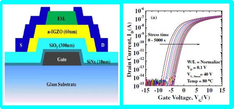
[Oxide semiconductor TFTs]
Japanese Journal of Applied Physics, 53, 08NG04 (2014)
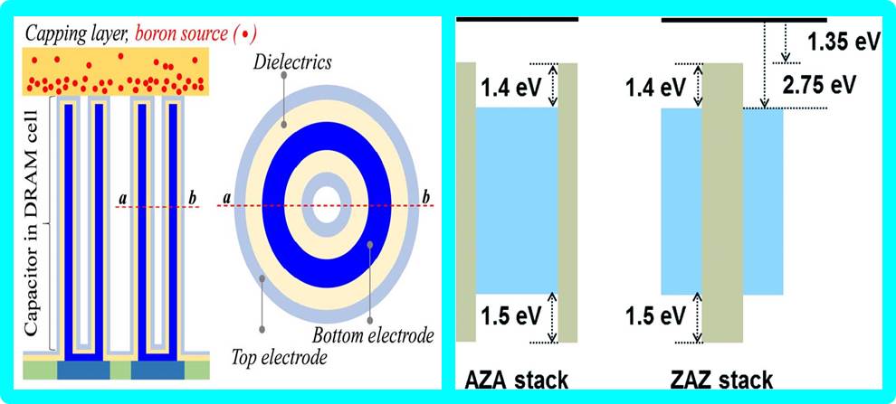
[MOS and MIM high-k capacitors]
IEEE Transactions on Electron Devices, 65, 4839 (2018)
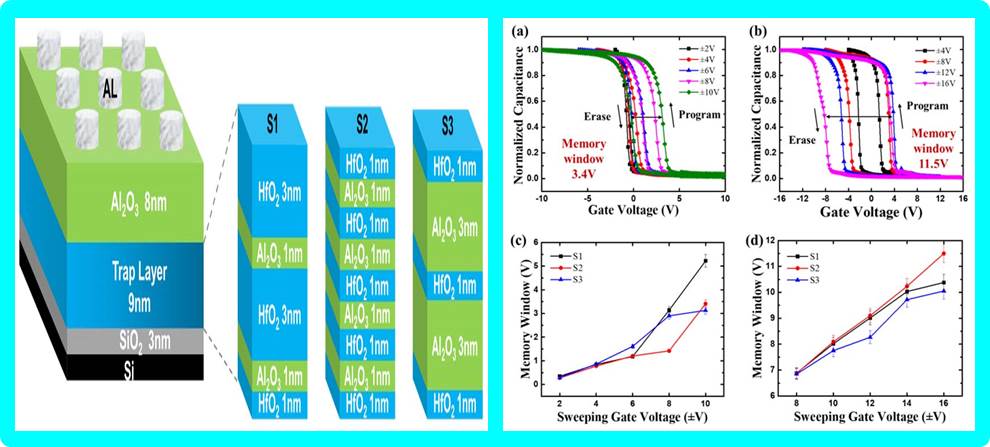
[Charge trap devices]
IEEE Electron Device Letters, 40, 1427 (2019) |
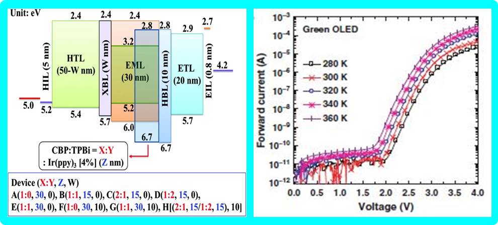
[OLEDs]
Journal of Nanoscience and Nanotechnology, 18, 5908 (2018)
[MOSFETs]
IEEE Transactions on Electron Devices, 65, 3237 (2018) |