


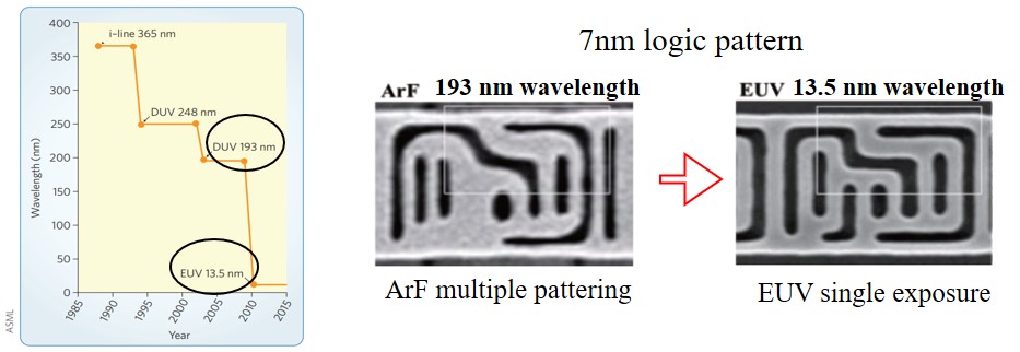
Lithography is the process of drawing a circuit with light, which is 60% of the processing time of a semiconductor. We have been working on a 193nm lithography process using ArF by 2010, but we are currently working on a 13.5nm lithography process using EUV. The purpose of using EUV is to reduce the width of semiconductor wirings because the cost of production is reduced and better semiconductors can be made. EUV is an abbreviation of Extrime Ultraviolet, and is a lithography technique using light having a short wavelength of 13.5 nm in the ultraviolet region. It is possible to process fine dimensions. EUV lithography is attempting to use because it is technically and economically advantageous because it reduces the wavelength, but there are several problems.
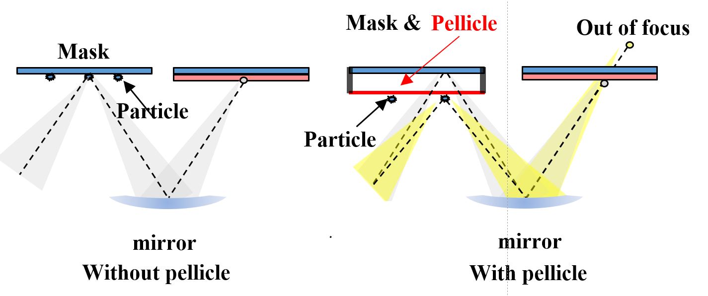
Several conditions are required to use EUV. One of them is the pellicle. The pellicle is used to reduce wafer defects resulting from mask contamination. A thin film having a high degree of transparency is placed at a certain distance from the mask surface, thereby causing the thin film to be contaminated instead of the mask surface. The pellicle currently has technical problems. The problem is that the EUV transmittance should be above 90%, the thermal properties should be good, the emissivity should be good, and the mechanical strength should be good.
We are currently studying graphite pellicles to solve the EUV pellicle problem. (We are also studying CNT as well as graphite.) We have developed a process to grow graphite to be defect-free, and there are many studies on pellicle.
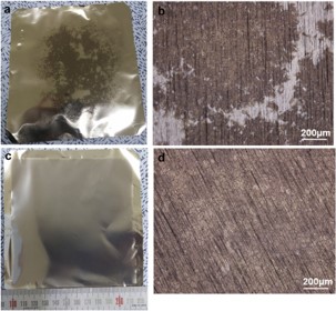
The above picture is Photographs and optical microscope images ofs NGF grown by two different processes. (a) Photograph and (b) optical image of NGF without intermediate cooling, G-870-120. (c) Photograph and (d) optical image of NGF with intermediate cooling, G-1035-10_750_870-100. (A colour version of this figure can be viewed online.)
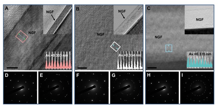
TEM cross-section image and the selected area electron diffraction (SAED) pattern of NGFs. (a-c) The NGFs were synthesized at 910°C, 925°C, and 1,000 °C. Each SAED pattern was collected using a 1.2μm aperture. The scale bar is 5nm. The selected area electron diffraction (SAED) patterns of (a)-(c) show a well-arranged layer structure (d)-(i).
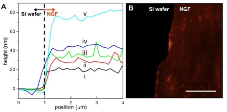
Thickness of nanometer-thick graphite film (NGF) measured by AFM. (A) AFM line profiles obtained at the edge of the NGF from 18 nm (i) to 78 nm (v). Each thickness was obtained after transfer of the NGF on to a Si wafer. (B) Typical AFM topographic image of NGF (34 nm thick). The scale bar of (B) is 5 ㎛
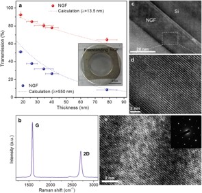
Transmission of a freestanding nanometer-thick graphite film (NGF), the Raman spectrum of NGF, and a high-resolution transmission electron microscopy (HRTEM) image. (a) EUV (λ = 13.5 nm) and visible light (λ = 550 nm) transmission of the NGF pellicle as a function of NGF thickness. The inset of (a) is a photo image of the pellicle (an 18 nm thick freestanding NGF) with a diameter of 10 mm. The red and blue dotted lines correspond to the simulations of transmission for EUV and visible light, respectively. (b) The representative Raman spectrum of NGF. (c) A cross-sectional TEM image of the thickness of 18 nm and (d) a well-arranged layer structure of the NGF. (e) HRTEM image of the NGF. The inset of (e) is the selected area electron diffraction (SAED) pattern of the NGF. The SAED pattern was collected using a 1.2 μm aperture.
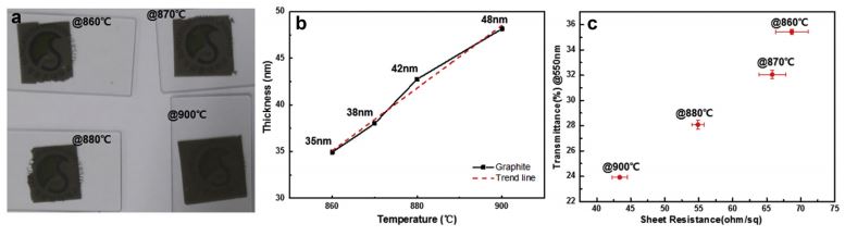
(a) Photograph of NGFs grown at different temperatures and transferred to a slide glass. (b) Thickness of NGF vs. growth temperature. (c) Relationship between transmittance and sheet resistance of NGFs grown at different temperatures.
The nanometer-thickness graphite film (NGF) synthesized by CVD has high thermal conductivity and good thermal and chemical stability. Moreover, it has a theoretical high EUV transmission (92% EUV transmission at a thickness of 18 nm) according to the EUV transmission equation TEUV. In our previous work, free-standing NGFs were applied to pellicles for EUVL. The large-scale NGFs were synthesized on Ni foils using the “one-stage” CVD process at 1035 ℃ (as shown in Fig. 1a), and the thickness of the as-grown NGF used for 50 X 50 mm pellicle fabrication was 86 ± 8 nm, which achieved an EUV transmission of 58 ± 3%. To obtain a higher EUV transmission, we reduced the thickness of NGF to 60 ± 6 nm (EUV transmission 68 ± 3%) by prolonged (120 min) oxygen plasma treatment (etching rate ~0.23 nm/min). However, the thickness distribution and uniformity of NGF may be changed after plasma treatment, which affects the quality of the pellicle. To fabricate a pellicle with high EUV transmission and uniformity, we improved our CVD process for the direct synthesis of thin large-area NGFs with excellent uniformity. In this paper, we describe a “two-stage” CVD process that includes an intermediate cooling step. Large-scale (120 X 120 mm) NGFs with a thickness of 38 nm were directly synthesized at a relatively lower growth temperature (870 ℃). The properties of NGF are analyzed and the mechanism of the “two-stage” CVD process is discussed.
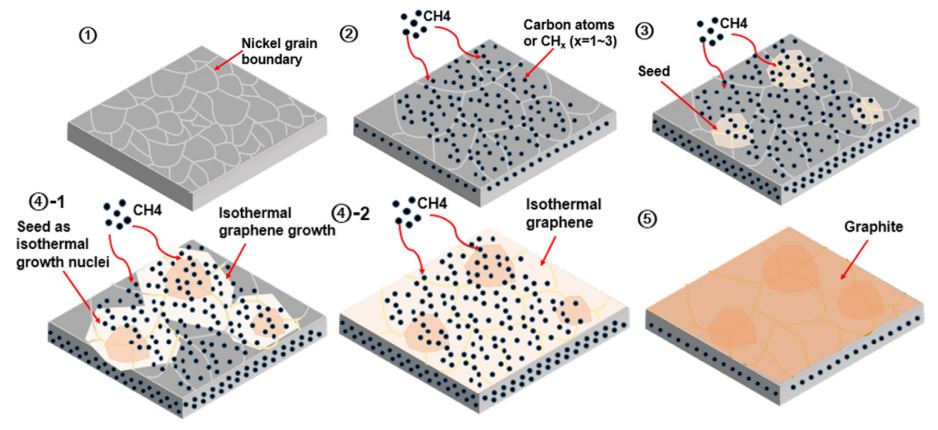
Schematic of the intermediate cooling growth process; steps ① to ⑤ correspond to the numbers in Figure.
In step ①, raw Ni foil with small grain is annealed at 1035 ℃ for 40 min and 100 sccm hydrogen is injected during the pre-annealing process. Preannealing is used for cleaning and rearranging the surface of the Ni foil to make it suitable for graphite growth. The grains of the Ni foil grow and recrystallize during this process. Hydrogen plays an important role in the CVD process from the start (cleaning and crystallization of the Ni substrate) to the end (passivation of graphene defects and other procedures). For step ②, 10.5 sccm of CH4 is injected into the chamber as the carbon precursor. Because of the high temperature (1035 ℃) of the substrate and the catalytic action of Ni, methane molecules easily attach to the surface of Ni and generate carbon atoms and CHx radicals. The carbon diffusion rate is so high that we can assume that most of the carbon atoms or clusters dissolved in the bulk of the Ni foil during this step. Large numbers of carbon atoms will be used for “seeds” formation during the intermediate cooling. Immediately after step ②, the Ni foil temperature is cooled to 750 ℃ within 2 min, and the intermediate cooling process begins (step ③). Because carbon solubility decreases at a lower temperature, the carbon atoms dissolved in the Ni foil in step ② will precipitate onto the surface through the grain boundaries and step edges and nucleate in the form of thin graphite flakes as the “seeds”. Step ④ is the main growth process for NGF. The substrate is heated to the growth temperature (860/870/880/900 ℃) and maintained for 100 min for isothermal growth. Normally, the nucleation during isothermal growth occurs when the concentration of carbon atoms in the Ni catalysts reaches the solubility limit of carbon in Ni and it requires a higher energy barrier (~1.5 eV) than that for the growth (~0.9 eV). However, by using the intermediate cooling process, we do not need to consider the energy barrier for nucleation because the seeds formed during the intermediate cooling can act as the nuclei for isothermal growth. During isothermal growth, the seeds attract not only the carbon atoms in the bulk of the Ni foil, but also the carbon atoms that diffuse on the surface of the Ni foil through the dissociation of methane molecules. Because of the uniform distribution of the seeds, isothermal film growth can start throughout the Ni foil and cover the entire Ni foil in the form of monolayer/fewlayer graphene. Finally, cooling occurs in step ⑤. With the decrease in solubility, large numbers of carbon atoms precipitate from the bulk of the Ni foil and form carbon layers under the isothermal graphene film. The full-sized isothermal film ensures that most of the precipitated carbon atoms can be directly used for NGF growth.
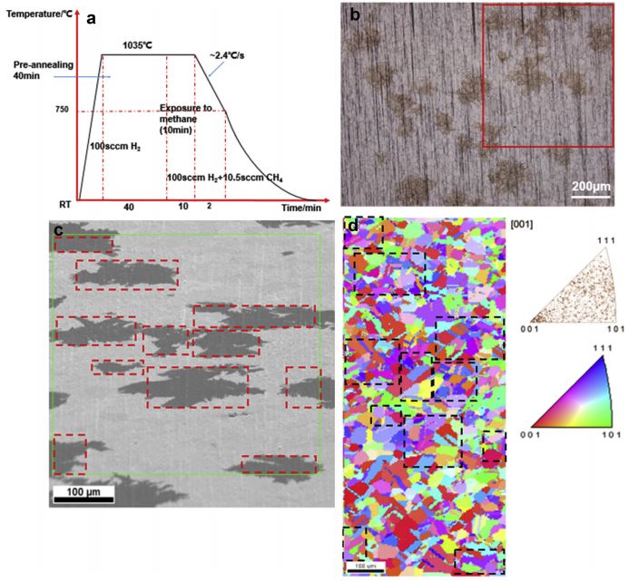
Intermediate cooling seed formation test. (a) Annealing line in the seed formation test. (b) Optical image of seeds (thin graphite flakes) on Ni foil. (c) SEM image of seeds on the Ni foil. (d) EBSD mapping of as-grown Ni foil; the scale bar is 100 mm.
